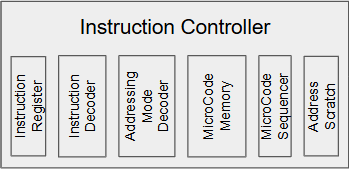
Designing the Instruction Controller
- Anthony Faulise
- Mar 31
- 5 min read

In my last post, I walked through the planning of the Instruction Controller. Please note that while re-reading that post to work on this next phase, I discovered an error I made. I have revised the previous post with a “Do-Over” section to call out my error and develop a corrected solution.
Also, during the design of the Instruction Controller, I identified another oversight. I failed to provide the Instruction Controller a way to select the Instruction Block to store the result of an instruction. The IC will need a way to force ID6-ID4 = 101 and route MLB3-0 to ID2-0. I can do this by controlling the high 3 bits of the AMD output according to an output from the IC state controller I will name FETCH_SAVE.
Now it’s time to do the actual design.
First, I built a state diagram to capture the sequence of events. The numbers in parentheses are the State IDs, which I use when I specify the contents of the state transition ROM.

The basic idea is that we start by asking the bus controller to fetch the next instruction. While we’re waiting for the instruction, we increment the PC. When the instruction becomes ready, we latch it in the Instruction Register and begin analyzing the value. A logic unit called the Operand Count Decoder determines whether the IR calls for a 2-operand, 1-operand, or 0-operand instruction. Based on that, we fetch the operand(s) we need, initiating each fetch and waiting for its completion. Once any required operands are fetched, we initiate execution of the instruction and then wait for its completion. When the instruction is completed, if there is a result to store, we store the result and wait for the store to complete. Finally, we circle back and request the next instruction.
As previously mentioned, how we go about fetching and saving instructions will depend on the addressing mode of the operand. It could range from something as simple as reading the Register RAM to something as complex as a doubly-indirect fetch where we use an address contained in a register to read a word in main memory and use that value as the address from which we read the actual operand. In each case, I will rely on a sequence of microcoded instructions to perform the fetch (or store) to (or from) the appropriate ALU operand latch, according to whether the operand is the first or second operand (or the result).
The major computations I presented in the previous post are:
Based on the IR, determine whether we have a 2-, 1-, or 0-operand instruction
Based on the IR, select the Instruction Group and route the remaining instruction bits to the lower end of the Instruction Decoder Address
Based on the IR bit fields for the selected operand (1 or 2), the Addressing Mode Decoder will determine which addressing mode to use and which bits from the operand field to route to the Register Address
The Instruction Controller has to do a few other things:
Latch the value from the bus controller’s data bus into the Instruction Register when an instruction is first loaded
Based on whether we want to perform microcode to fetch an operand or perform microcode to perform the instruction itself, route either the Addressing Mode Decoder output or the Instruction Group Decoder output to the Instruction Decoder ROM
Based on whether we are fetching Operand 1 or Operand 2, route the operand field of the IR to the Addressing Mode Decoder
When fetching the Program Counter, route the address of the PC register (0x20) to the Register Address bus
Determine, jointly with the MicroCode, what to load into the MicroCode Program Counter
The output of the Instruction Decoder ROM as the start of the next MicroCode routine
The constant 0x0000 in case of RESET
A value previously stored by the microprogram, in case of a branch in the MicroCode
One plus the previous value of the MicroCode PC, when we just want to advance to the next MicroCode instruction
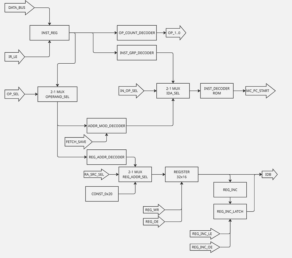
Here’s the big picture:

Just to clarify the block names:
INST_REG - instruction register, latches the instruction word (IW)
OP_COUNT_DECODER - Operand Count Decoder - based on the IW determines if we have 0, 1, or 2 operands
INST_GRP_DECODER - Instruction Group Decoder - based on the IW, determines the Instruction Group, which in turn sets the top bits of the Instruction Decoder address (ID6-4) and routes the appropriate bits from the IW to the lower part of the Instruction Decoder address ID3-0)
OPERAND_SEL - Operand Selector - selects which operand field from the IW to pass to the Address Mode Decoder and Register Address Decoder
ADDR_MOD_DECODER - Addressing Mode Decoder - examines the selected operand field from the IW and determines the addressing mode, based on which, passes the appropriate bits from the operand field to the Instruction Decoder Address selector
FETCH_SAVE - Controls the high bits of the ADDR_MOD_DECODER output to select the MicroCode instructions to fetch or save an operand according to the operand Addressing Mode
REG_ADDR_DECODER - Register Address Decoder - passes bits from the selected operand field to the Register Address register
REG_ADDR_SEL - Register Address Selector - selects which address to pass to the Register RAM
IDA_SEL - Instruction Decoder Address Selector - passes the Instruction Group Decoder output or the Addressing Mode Decoder output to the Instruction Decoder ROM to look up the MicroCode starting address either for the main instruction or for the routine to fetch / store the operand
INST_DECODER_ROM - Instruction Decoder ROM - based on the instruction or the addressing mode, looks up the starting address in the MicroCode ROM for the routine to process the instruction or fetch / store the operand
MC_PC_SEL - MicroController Program Counter Select - selects which address to load into the MicroCode Program Counter: the lookup from the Instruction Decoder, 0x0000 (for RESET), the MC_JMP_REG (used for MicroCode branching), or the MC_PC_INC register (used to increment the MicroCode Program Counter value for stepping through MicroCode)
MC_PC - MicroCode Program Counter - the address in the MicroCode ROM of the currently executing MicroCode instruction
MC_JMP_REG - MicroCode Jump Register - when MicroCode needs to branch, it loads the target address in the MC_JMP_REG then performs the branch test. If the branch condition is met, the MC_JMP_REG is loaded into the MC_PC, otherwise the MC_PC advances to the next MicroCode instruction
MC_PC_INC - MicroCode Program Counter Increment - adds 1 to the current output of the MicroCode Program Counter, used to advance the MC_PC by one when executing MicroCode
The state machine will need to generate a suite of control signals to orchestrate the different parts of the Instruction Controller. Based on the diagram above, the control signals will be:
IR_LE - Instruction Register Latch Enable
IN_OP_SEL - Instruction / Operand Select (for the Instruction Decoder ROM Address bus)
OP_SEL - Operand Select (to route IR bit fields for operand 1 or 2 to the Address Mode Decoder)
FETCH_SAVE - Operand Fetch/Save
RA_SRC_SEL - Register Address Source Select (to select the output of the Register Address Decoder when fetching an operand or to select the Program Counter register (32 = 0x20)
REG_WR - Register Write
REG_OE - Register Output Enable
REG_INC_LE - Register Incrementer Latch Enable
REG_INC_OE - Register Incrementer Output Enable
MC_SRC_SEL1..0 - MicroCode Program Counter Source Select Bits 1, 0
MC_PC_LE - MicroCode Program Counter Latch Enable
MC_START - MicroCode Start
MREQ - to the bus controller
M_READ - to the bus controller
The state machine will receive the following inputs:
Instruction Ready
MicroCode Done
OP_1..0 - Operand Count Bits 1, 0
Clock
Reset
My next step will be the actual circuit design of the Instruction Controller.

Comments