Planning the Instruction Controller
- Anthony Faulise
- Mar 17
- 14 min read
Updated: Apr 1
Lookout! On 3/26, while working on the design of the Instruction Controller, I discovered an error in my logic in this post. I've pasted in a correction. Look for "Do Over."
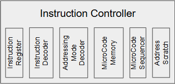
Today, I’m going to focus on the CPU Instruction Controller. The Instruction Controller will orchestrate its subsystems to fetch an instruction, get any needed operands, perform the instruction itself, potentially store a result, and queue up the next instruction.
Full disclosure, this post is the result of a week or two of thinking, note taking, and revising.
Overview
My initial vision of the Instruction Controller (IC) is a sequencer that will:
Load the PC to the Address Latch
Ask the Bus Controller to fetch an instruction and store it in the Instruction Register
Have the Addressing Mode Decoder examine the Instruction Register to see if we need an operand, or skip to 7.
Load the MicroCode PC with the start address of the routine to fetch the first operand according to the Addressing Mode. The MicroCode Sequencer will execute until the first operand is stored in the appropriate ALU latch.
Have the Addressing Mode Decoder examine the Instruction Register again to see if we need an additional operand, or skip to 7, leaving any computed or fetched indirect address in the Address Scratch register.
Load the MicroCode PC with the start address of the routine to fetch the second operand according to the Addressing Mode. The MicroCode Sequencer will execute until the second operand is stored in the appropriate ALU latch. This step will potentially overwrite the computed or fetched indirect address in the Address Scratch register with a new address, which will serve as the destination of the result, if appropriate.
Have the Addressing Mode Decoder examine the Instruction Register again and route the appropriate bits to the Instruction Decoder.
The Instruction Decoder looks up the start address of the MicroCode routine for the subject instruction.
The Controller turns control over to the MicroCode Sequencer, which executes the necessary instructions to perform the actual data manipulation. The MicroCode will store the result of any computation, possibly making use of the address in the Address Scratch register or the Register Address latch, before returning.
When the MicroCode signals it is done, the Controller will then return to step 1 above.
Since the MicroCode for the actual instruction may take several cycles, I thought I might try to pipeline operations a little and start the instruction fetch and Addressing Mode Decoder steps as soon as the Controller turns control over to the MicroCode Sequencer for the instruction itself. Whoever finishes first would have to wait.
Hmm. It sounds nice, but as I type this I see a potential problem. If the result of the current instruction alters one of the operands of the subsequent instruction, that would be a problem. In theory, I could check to see if the addresses are the same and then pause the pre-fetch logic if they are, or even detect if the operand >changed<. Or it could be more trouble than it’s worth. I’m voting for the latter.
Maybe the Controller could at least pre-fetch the next instruction. Ah, but what if there’s a branch? I could pre-fetch the instruction as long as the current instruction isn’t a branch, jump, RTS, RTI, etc. OK, KISS for now.
Allright, in any case, I see the Instruction Sequencer (IS) using a shift register to sequence the steps as:
Route PC to AR, fetch instruction to IR, evaluate IR with AMD logic on the fly, preload the IS if needed to jump ahead to 3 or 4
Load Operand 2 (src) to ALU-Left, evaluate IR with AMD logic on the fly
Load Operand 1 (dest / src+dest) to ALU-RIGHT
Start here for 1-operand instructions
Lookup Instruction MC Start Address
Start here for 0-operand instructions
Start MC for instruction processing
Instruction processing is responsible for writing result of any instruction to dest
Instruction processing is responsible for incrementing PC
When instruction MC is done, signal IS to jump back to 1
Addressing Mode Decoder
The Addressing Mode Decoder (AMD) unit needs to do a few computations:
Examine the instruction and determine the number of operands, this decides when to turn control over to the instruction MicroCode and which ALU input latch each operand is routed to
Examine an operand field (6-bits) and determine the MicroCode start address for the routine to handle fetching the operand
Examine an operand field (6-bits) and determine how to route some of the operand field bits to the Register Address bus
For certain instructions, IM, SWI, BRA, JMP, JSR, latch or gate some of the operand-field bits to make them available to the MicroCode.
Examine the IR and route appropriate bits to the Instruction Decoder to determine the MicroCode start address for the actual instruction itself.
Let’s look at each computation in turn.
Number of Operands
There are fifteen permitted instructions that require two operands. I’ve designed these so that if the high 4 bits of the IR are 0000 - 1110, there are 2 operands.
If the high 4 bits of the IR are 1, then we examine the next 6 bits, IR11 - IR6. If they are 000000 - 001111, we have a 1-operand instruction.
If IR11-IR10 are 01 or 1X, we have 0-operand instruction, but we need to parse the OpCode bits in a special way.
Finally, if IR15-IR6 are 1, then we have a 0-operand instruction without special treatment of the operand field.
Two Operand = NAND(IR15-IR12) = OR(IR15*, IR14*, IR13*, IR12*)
One Operand = AND(IR15, IR14, IR13, IR12, IR11*, IR10*)
Zero Operand = AND(IR15, IR14, IR13, IR12, B11) OR AND(IR15, IR14, IR13, IR12, IR10)
Each of these expressions has 2 gate delays, which is the best we can do.
Operand Fetch MicroCode Start Address
To actually fetch the operand and latch it in a register or one of the two ALU operand latches, we will turn control over to the MicroCode. There will be a separate MicroCode routine to handle each Addressing Mode. We need to examine the Addressing Mode and determine the start address in MicroCode to handle it. That is this task.
We will use a small ROM to examine the addressing mode bits and lookup the MicroCode starting address. In principle, we could just route all 16 bits of the IR to the Instruction Decoder to find the start address, but because there is so much redundancy, that is inefficient. We would need a 64Kx16 memory to look up just 8 distinct Addressing Modes. Better to reduce it with some logic.
Note that we’ll need to do this for each operand, so we’ll need logic to select the Addressing Mode select bits for each of the operands in sequence when we have two operands, and just for the one operand when we have just one.
As a reminder, here are the addressing modes and how the bits of the Operand field signal the mode.
Mode Name | OP5 | OP4 | OP3 | OP2 | OP1 | OP0 | Addr Mode ID |
Register | 0 | X | X | X | X | X | 0 = 000 |
Indexed | 1 | 0 | 0 | X | X | X | 1 = 001 |
Indirect | 1 | 0 | 1 | X | X | X | 2 = 010 |
Doubly Indir | 1 | 1 | 0 | X | X | X | 3 = 011 |
Indir Pre-Dec | 1 | 1 | 1 | 0 | X | X | 4 = 100 |
Indir Post-Inc | 1 | 1 | 1 | 1 | X | X | 5 = 101 |
Immediate | 1 | 1 | 1 | 1 | 1 | 1 | 6 = 110 |
We’ll map the OP bits to the Addressing Mode ID to look up the MC start address of the routine to handle the Addressing Mode. We need to generate a 3-bit value. Here are the Karnaugh maps to generate the low 3 bits of the MC start-address lookup. We’ll deal with the upper bits later.
Mode Lookup Bit 2 | OP2-0: 000 | 001 | 011 | 010 | 110 | 111 | 101 | 100 |
OP5-3: 000 | 0 | 0 | 0 | 0 | 0 | 0 | 0 | 0 |
001 | 0 | 0 | 0 | 0 | 0 | 0 | 0 | 0 |
011 | 0 | 0 | 0 | 0 | 0 | 0 | 0 | 0 |
010 | 0 | 0 | 0 | 0 | 0 | 0 | 0 | 0 |
110 | 0 | 0 | 0 | 0 | 0 | 0 | 0 | 0 |
111 | 1 | 1 | 1 | 1 | 1 | 1 | 1 | 1 |
101 | 0 | 0 | 0 | 0 | 0 | 0 | 0 | 0 |
100 | 0 | 0 | 0 | 0 | 0 | 0 | 0 | 0 |
Mode Lookup Bit 1 | OP2-0: 000 | 001 | 011 | 010 | 110 | 111 | 101 | 100 |
OP5-3: 000 | 0 | 0 | 0 | 0 | 0 | 0 | 0 | 0 |
001 | 0 | 0 | 0 | 0 | 0 | 0 | 0 | 0 |
011 | 0 | 0 | 0 | 0 | 0 | 0 | 0 | 0 |
010 | 0 | 0 | 0 | 0 | 0 | 0 | 0 | 0 |
110 | 1 | 1 | 1 | 1 | 1 | 1 | 1 | 1 |
111 | 0 | 0 | 0 | 0 | 0 | 1 | 0 | 0 |
101 | 1 | 1 | 1 | 1 | 1 | 1 | 1 | 1 |
100 | 0 | 0 | 0 | 0 | 0 | 0 | 0 | 0 |
Mode Lookup Bit 0 | OP2-0: 000 | 001 | 011 | 010 | 110 | 111 | 101 | 100 |
OP5-3: 000 | 0 | 0 | 0 | 0 | 0 | 0 | 0 | 0 |
001 | 0 | 0 | 0 | 0 | 0 | 0 | 0 | 0 |
011 | 0 | 0 | 0 | 0 | 0 | 0 | 0 | 0 |
010 | 0 | 0 | 0 | 0 | 0 | 0 | 0 | 0 |
110 | 1 | 1 | 1 | 1 | 1 | 1 | 1 | 1 |
111 | 0 | 0 | 0 | 0 | 1 | 0 | 1 | 1 |
101 | 0 | 0 | 0 | 0 | 0 | 0 | 0 | 0 |
100 | 1 | 1 | 1 | 1 | 1 | 1 | 1 | 1 |
So:
MLookupBit2: OP5 AND OP4 AND OP3
MLookupBit1: AND(OP5, OP4, OP3*) OR AND(OP5, OP4*, OP3) OR AND(OP5, OP4, OP3, OP2, OP1, OP0)
MLookupBit0: AND(OP5, OP4, OP3*) OR AND(OP5, OP4*, OP3*) OR AND(OP5, OP4, OP3, OP2, ,OP1, OP0*) OR AND(OP5, OP4, OP3, OP2, OP1*)
Register Address Bit Routing
For most of the addressing modes, I need to route register select information from the operand field to the register memory address lines (RA). Most of the development for this topic is in the post “Instruction Set and CPU Architecture.”
The logic is:
RA4 = OP5 OR OP4
For RA3:
Conceptually:
RA3 | OP2, 1, 0: 000 | 001 | 011 | 010 | 110 | 111 | 101 | 100 |
OP5, 4, 3: 000 | OP3 | OP3 | OP3 | OP3 | OP3 | OP3 | OP3 | OP3 |
001 | OP3 | OP3 | OP3 | OP3 | OP3 | OP3 | OP3 | OP3 |
011 | OP3 | OP3 | OP3 | OP3 | OP3 | OP3 | OP3 | OP3 |
010 | OP3 | OP3 | OP3 | OP3 | OP3 | OP3 | OP3 | OP3 |
110 | OP2 | OP2 | OP2 | OP2 | OP2 | OP2 | OP2 | OP2 |
111 | 1 | 1 | 1 | 1 | 1 | 1 | 1 | 1 |
101 | OP2 | OP2 | OP2 | OP2 | OP2 | OP2 | OP2 | OP2 |
100 | OP2 | OP2 | OP2 | OP2 | OP2 | OP2 | OP2 | OP2 |
In detail:
RA3 | OP2, 1, 0: 000 | 001 | 011 | 010 | 110 | 111 | 101 | 100 |
OP5, 4, 3: 000 | 0 | 0 | 0 | 0 | 0 | 0 | 0 | 0 |
001 | 1 | 1 | 1 | 1 | 1 | 1 | 1 | 1 |
011 | 1 | 1 | 1 | 1 | 1 | 1 | 1 | 1 |
010 | 0 | 0 | 0 | 0 | 0 | 0 | 0 | 0 |
110 | 0 | 0 | 0 | 0 | 1 | 1 | 1 | 1 |
111 | 1 | 1 | 1 | 1 | 1 | 1 | 1 | 1 |
101 | 0 | 0 | 0 | 0 | 1 | 1 | 1 | 1 |
100 | 0 | 0 | 0 | 0 | 1 | 1 | 1 | 1 |
RA3 = AND(OP5, OP4, OP3) OR AND(OP5*, OP3) OR AND(OP5, OP2)
For RA2:
Conceptually:
RA2 | OP2, 1, 0: 000 | 001 | 011 | 010 | 110 | 111 | 101 | 100 |
OP5, 4, 3: 000 | OP2 | OP2 | OP2 | OP2 | OP2 | OP2 | OP2 | OP2 |
001 | OP2 | OP2 | OP2 | OP2 | OP2 | OP2 | OP2 | OP2 |
011 | OP2 | OP2 | OP2 | OP2 | OP2 | OP2 | OP2 | OP2 |
010 | OP2 | OP2 | OP2 | OP2 | OP2 | OP2 | OP2 | OP2 |
110 | OP2* | OP2* | OP2* | OP2* | OP2* | OP2* | OP2* | OP2* |
111 | 1 | 1 | 1 | 1 | 1 | 1 | 1 | 1 |
101 | OP2* | OP2* | OP2* | OP2* | OP2* | OP2* | OP2* | OP2* |
100 | OP2* | OP2* | OP2* | OP2* | OP2* | OP2* | OP2* | OP2* |
In detail:
RA2 | OP2, 1, 0: 000 | 001 | 011 | 010 | 110 | 111 | 101 | 100 |
OP5, 4, 3: 000 | 0 | 0 | 0 | 0 | 1 | 1 | 1 | 1 |
001 | 0 | 0 | 0 | 0 | 1 | 1 | 1 | 1 |
011 | 0 | 0 | 0 | 0 | 1 | 1 | 1 | 1 |
010 | 0 | 0 | 0 | 0 | 1 | 1 | 1 | 1 |
110 | 1 | 1 | 1 | 1 | 0 | 0 | 0 | 0 |
111 | 1 | 1 | 1 | 1 | 1 | 1 | 1 | 1 |
101 | 1 | 1 | 1 | 1 | 0 | 0 | 0 | 0 |
100 | 1 | 1 | 1 | 1 | 0 | 0 | 0 | 0 |
RA2 = AND(OP5, OP4, OP3) OR AND(OP5*, OP2) OR AND(OP5, OP2*)
For RA1 and RA0:
RA1 = OP1
RA0 = OP0
Special Bits Capture
See below.
Instruction Start Address Lookup
We will use a small ROM (the Instruction Decoder, ID) to look up the starting address in the MicroCode to either fetch an operand or to perform an instruction. We don’t yet know how many address lines we’ll need to select from the ID, but let’s refer to them as IDA0, IDA1, …
To conserve resources, we would like the lookups in the ID to be relatively compact, meaning that there should not be large groups of input addresses that are unused. That just wastes ROM real-estate.
For operand fetch, we use logic to map the Addressing Mode to 3 bits: MLookupBit2, 1, and 0
Map MLB2 to IDA2, MLB1 to IDA1, MLB0 to IDA0.
We’ll have to figure out IDA3… later
For 2-operand instructions, we can route IR15-IR12 to IDA3-IDA0
We’ll have to figure out IDA4… later
For 1-operand instructions, we can route IR9-IR6 to IDA3-IDA0
We’ll have to figure out IDA4… later
For most 0-operand instructions, we can route IR3-IR0 to IDA3-IDA0
For 0-operand instructions IM, SWI, BRA, JMP, and JSR, we will want to find a way to map to IDA3-IDA0 as well
I haven’t mentioned it yet, but I’ll also need some routines in the MicroCode to store the result of instruction operations according to the addressing mode of the destination operand (or the single operand). I can probably reuse MLB2-MLB0, but will need to map the options to a different block of the ID.
Of course, we can see that we will need to generate the upper bits of IDA to avoid collisions among the different groups of instructions that all want to use IDA3-IDA0. The 2-, 1-, and 0-operand instructions all want 4-bits each, so let’s allocate 16 addresses to each major block, and map the blocks as follows:
Lookup Type | IDA6-IDA4 | IDA3-IDA0 |
Operand Fetch | 000 | 0, MLB2, MLB1, MLB0 |
2-Operand Instruction | 001 | IR15, IR14, IR13, IR12 |
1-Operand Instruction | 010 | IR9, IR8, IR7, IR6 |
0-Operand Instruction | 011 | IR3, IR2, IR1, IR0 |
Special 0-Operand | 100 | (Logic Mapping) |
Result Save | 101 | 0, MLB2, MLB1, MLB0 |
Unused | 110 | n/a |
Reserved | 111 | (Logic Mapping) |
Bottom line: I need 128 addresses in the IM. The width of the IM will be determined by the size of the MicroCode ROM, which we don't yet know.
As I was typing this out, it occurred to me that I could use the “Reserved” block of lookups (IDA6-4: 111) to lookup MicroCode to handle RESET, and Interrupt handling. I’ll keep that in my back pocket for later.
Finally, I need to design some logic to map the special 0-operand instructions (IW, SWI, BRA, JMP, JSR) to a compact list of values for IDA3-IDA0. Let’s tackle that.
Instruction | IR | Desired IDA3-0 |
IM | 1111 0100 00mm mmmm | 0000 |
SWI | 1111 0100 01mm mmmm | 0001 |
BRA | 1111 1ccc dddd dddd | 0010 |
JMP | 1111 1111 1110 0ccc | 0011 |
JSR | 1111 1111 1110 1ccc | 0100 |
I observed two possible optimizations here.
First, if I reorganize the bits of BRA to move the condition codes to the low bits, it will make it easier to use the condition code bits because they will always be in the same place and I won’t need logic to select them from two different places.
Second, if I set the desired IDA for JMP and JSR differently, I can map IR3 to IDA0 to differentiate between JMP and JSR with less logic. Using the same observation, I see that I can likely map IR6 to IDA0 to differentiate between IM and SWI.
OK, so here’s the redesigned map for IDA3-0.
Instruction | IR | Desired IDA3-0 |
IM | 1111 0100 00mm mmmm | 0000 |
SWI | 1111 0100 01mm mmmm | 0001 |
BRA | 1111 1ddd dddd dccc | 0010 |
JMP | 1111 1111 1110 0ccc | 0100 |
JSR | 1111 1111 1110 1ccc | 0101 |
I didn't bother with a Karnaugh map on this one, just eyeballed it. Here’s the logic to control the IDA3-0 and the routing of the bit fields for ccc, dddd dddd, and mmm mmm.
IDA3 = 0
IDA2 = AND(IM15-IM5, IM4*)
IDA1 = AND(IM15-11)
IDA0 = AND(IM15-IM12, IM11*, IM10, IM9*, IM8*, IM7*, IM6) OR AND(IM15-IM5, IM4*, IM3)
MMMGate = AND(IM15-12, IM11*, IM10, IM9*, IM8*, IM7*)
DDDGate = AND(IM15-11)
CCCGate = AND(IM15-IM5, IM4*)
At the cost of one additional gate of propagation delay, it would be possible to re-use AND(IM15-IM12), AND(IM11*, IM10, IM9*, IM8*, IM7*), and AND(IM11-IM5). Also note that some of the ANDs are so wide that I will have to cascade two AND gates.
Whoopsie! Do-Over Required
[Edit 3/26/25: I am such a numbskull. The design above won’t work! I can’t believe I didn’t see the problem. This is embarrassing.
Clearly, there are values of dddd dddd and ccc that make BRA indistinguishable from JMP and JSR. That means the instruction decoder can’t tell which instruction to execute. That’s a problem.
I need to reassign the distinguishing upper bits of the third hex digit from the right of the Instruction Word so that the Instruction Decoder can distinguish between the instructions, regardless of what the operand is.
Since BRA needs the most auxiliary bits, let me start fixing it by making the op code for BRA:
1111 0ddd dddd dccc
Then Special Instructions IM, SWI, JMP, and JSR can be (respectively):
1111 1000 00 mmm mmm
1111 1000 01 mmm mmm
1111 1000 10 000 ccc
1111 1000 11 000 ccc
This approach keeps the bits that distinguish the instruction class all together and clusters the bits that differentiate the specific instruction within the class all together too.
The standard 1-Operand instructions can be:
1111 11xx xxpp pppp
Where xxxx encode one of 16 instructions, which should be enough
pp pppp encode the operand
Finally, Zero-Operand instructions can be:
1111 111111 00 xxxx
To summarize:
Instruction Word | Instruction | ID6-ID4 | Instruction / Instruction Group |
0000 aaaaaa bbbbbb
| LD, ADC, ADD, AND, CMP, OR, SUB, SBC, XOR | 001 | 2-operand instructions |
1111 0 dddddddd ccc | BRA | 100 | Special |
1111 100000 mmmmmm
| IM | 100 | Special |
1111 100001 mmmmmm
| SWI | 100 | Special |
1111 100010 000ccc | JMP | 100 | Special |
1111 100011 000ccc | JSR | 100 | Special |
1111 110000 bbbbbb
| NOT, NEG, INC, DEC, ROT*, SHIFT* | 010 | 1-operand instructions |
1111 111111 00 0000
| RTS, SWI, RTI, NOP, STC, CLC, etc. | 011 | 0-operand instructions |
aaaaaa = Source operand bits
bbbbbb = Destination operand bits
ccc = Condition code for branches and conditional jumps
dddddd = Displacement (-128 - +127) for relative branches
mmmmmm = bit mask for interrupts
OK, now that seems to be sorted, let me rebuild the logic that will detect the instruction group (for the high bits of the Instruction Decoder) and route the bit fields that distinguish the specific instructions to the low bits of the Instruction Decoder.
Here is the logic for the high bits of the Instruction Decoder lookup table.
Note that ID6-4 = 000 means we are looking up the subroutine to fetch an operand according to the Addressing Mode. The Instruction Sequencer state machine will force ID6-ID4 = 000 during those states and will drive ID3-ID0 from the Addressing Mode Decoder.
ID6 = AND(IW15, IW14, IW13, IW12, IW10*) OR
AND(IW15, IW14, IW13, IW12, IW11, IW10*)
(BY observation)
ID5 = AND(IW15, IW14, IW13, IW12, IW11, IW10, IW9*) OR
AND(IW15, IW14, IW13, IW12, IW11, IW10, IW9, IW8, IW7, IW6, IW5*, IW4*)
(By Karnaugh map)
ID4 = NAND(IW15, IW14, IW13, IW12) OR
AND(IW15, IW14, IW13, IW12, IW11, IW10, IW9, IW8, IW7, IW6, IW5*, IW4*)
(By observation)
Let’s see how I will route the instruction bits to the low bits of the ID.
Instruction Group | ID6-ID4 | Source for ID3-ID0 |
Operand Fetch | 000 | AMD |
2-Operand | 001 | IR15-IR12 |
1-Operand | 010 | IR9-IR6 |
0-Operand | 011 | IR3-IR0 |
I’ll use four 4-1 multiplexers to do this. I’ll need to select parts with an Output Enable function so I can suppress the outputs when ID6-ID4 is 100.
For the Special instructions, there is no “instruction field” in the IW, so we need to synthesize a compact set of values for ID3-ID0 based on the IR bits.
First, I lay out the table of the information I have to work with. Reflecting, I can see that bits IW9-6 map directly to the instruction, except for BRA.
Instruction Word | Instruction | ID3-ID0 |
1111 0 dddddddd ccc | BRA | xxxx |
1111 100000 mmmmmm
| IM | 0000 |
1111 100001 mmmmmm
| SWI | 0001 |
1111 100010 000ccc | JMP | 0010 |
1111 100011 000ccc | JSR | 0011 |
So, I could implement a little logic to map BRA to a value like 0100 and I’d be set.
ID3 = 0
ID2 = AND(IW11*, IW10*) OR
AND(IW11*, IW10)
ID1 = AND(IW11, IW10*, IW9*, IW8*, IW7)
ID0 = AND(IW11, IW10*, IW9*, IW8*, IW6)
I generated these with four Karnaugh maps for ID3, ID2, ID1, and ID0 with inputs: IW11, 10, 9, 8, 7, 6.
I can probably wire-OR these to the outputs of the 4-1 multiplexers I mentioned above, or use a buffer with a tri-state output.
END OF THE DO-OVER
One Final Comment
At the start of the project, I set as one of my objectives to use only TTL. I’m seeing now that using PLDs (22V10, 16V8, etc.) will reduce my chip-count (and wiring work) by a LOT. I think I’m going to back down on my initial commitment not to use PLDs. And, I’ve never used one before, so that will be fun.
Comentarios